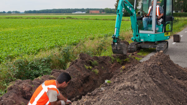

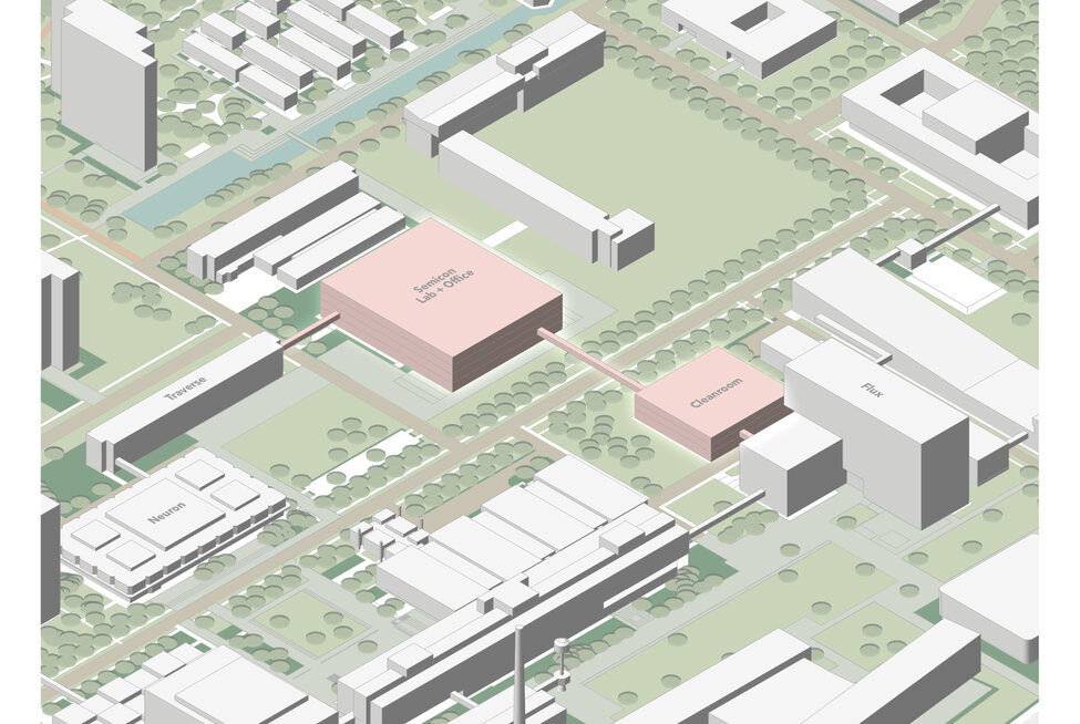
The Eindhoven University of Technology (TU/e) is to spend €200m building a laboratory and a cleanroom to support the Netherlands’ semiconductor industry.
The 5,000-sq-m building will house labs and classrooms. Its 1,200-sq-m cleanroom will have facilities for making chips.
It will let the university offer 2,000 graduate-degree places in engineering, applied physics and computer science.
Silvia Lenaerts, TU/e’s rector, said the projects would help Eindhoven to meet “the huge demand for top-tier engineering talent”.
The investment is part of TU/e’s recent “Future Chips” programme, aimed at making the Netherlands a centre of semiconductor technology.
It is also aimed at furthering “Project Beethoven”, a Dutch initiative to retain ASML, a company that makes state-of-the-art ultraviolet lithography machines, and is Europe’s main claim to be at the forefront of chip tech.
The government sees ASML as crucial to the economic future of the entire country. At present it employs 21,000 people, 40% of whom have moved from universities in other countries.
ASML believes its growth depends on the availability of highly skilled workers, and that its presence in the Netherlands depends on being able to find the workers it needs in the local labour market.
The expansion follows a decision by ASML to invest €80m over the next decade in joint research initiatives at TU/e. These will focus on plasma physics, mechatronics (that is, equipment for advanced manufacturing) optics and AI.
Work on the buildings will begin next year.
- Subscribe here to get stories about construction around the world in your inbox three times a week
Further reading: